NoGaPiG

Power Indicator/Guard
Board Version A, Document Version 2.2
Board Version A, Document Version 2.2
 |
A project to protect your QRP rig!
|
Safety First!
This project was developed after several experiences with "smoking" QRP rigs due to overcurrent, overvoltage and/or reverse voltage. Remember that gel cell batteries, power supplies and the like can supply tremendous amounts of current instantaneously. Take all steps necessary to avoid shorting the power leads from any large current supply. A dead-short can easily generate enough heat to melt the insulation of the supply leads and cause a fire. Even at low voltages, the amount of current available from these supplies can cause serious injury.
The NoGaPiG is designed to catch these conditions under normal operations. This does present a little problem during construction, since to be confident that it will perform as expected, you must test that the circuit actually catches these conditions. Even more so than with most projects, your best defense is to BE CAREFUL. If you're tired or in a hurry you should suspend your assembly and testing and pick it up after you're more rested.
This project has undergone extensive testing and review and should perform as expected. Several licensed amateur radio operators have successfully constructed it following these instructions. You are responsible for the proper construction, testing and operation of this device prior to its use or connection to other equipment.
All these items will be used later so just put them aside until the instructions call for them.
| C1 | .1uf bypass for U1 | ||
| D1 | 1N5231, 5.1v 500 mW Zener Reference for the OpAmp | ||
| D2 | 1N5245, 15v 500 mW Zener (Overvoltage Reference) | ||
| D3 | LED 2.1v 20 mA (Low Voltage Indicator)**Note: incorrectly marked D2 on PC board silk-screen | ||
| D4 | 1N5400 3A, 50v (Reverse voltage Crowbar) | ||
| F1 | PolySwitch 1.35A RXE135 | ||
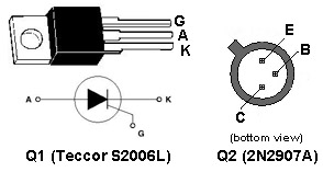
| Q1 | Teccor S2006L (SCR 6-8A capacity rating,gate trigger on 2-4v @ 30mA) | ||
| Q2 | 2N2907A PNP Switch to trigger SCR | ||
| R1 | 1.8K 1/4 w (Current Limiter for 5.1v Zener) | (brown,gray,red) | |
| R2 | 560 ohm 1/4 w for current limit for LED | (green,blue,brown) | |
| R3 | 10K 1/4 w (note: R3/R4 form voltage divider for threshold set) | (brown,black,orange) | |
| R4 | 8.2K 1/4 w (note: R3/R4 form voltage divider for threshold set) | (gray,red,red) | |
| R5 | 820 ohm 1/4w current limiter for 15v Zener | (gray,red,brown) | |
| R6 | 100 ohm 1/4 w Current Limiter for SCR gate | (brown,black,brown) | |
| R7 | 150 ohm 1/4 w Current limiter for Q2 | (brown,green,brown) | |
| U1 | LM311N Low Current OpAmp Voltage Comparator | ||
| PC Board (ver. A) | |||
| 1 8-pin DIP socket | |||

Note: D3 is incorrectly silk-screened as "D2" on the circuit board.
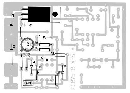
Step 0 - Using page 5 parts layout as a guide, orient PC board with Q1 SCR in the upper left hand corner of the board and D4 and F1 towards the left side of the board. All board references going forward will have this orientation.
Step 1 - Identify the PolySwitch (Resettable Fuse) and install it in the indicated mounting holes. Since there are several sizes of the devices you will have to carefully bend the leads to confirm to the holes and the unit you have. The fuse can be installed with either lead towards the supply voltage. These are rugged devices but avoid damaging the coating and device itself. Keep a short distance between the lead bend and the body of the device, about the width of the tips of a needle nosed pliers.
Step 2 - Identify D4 the 3A Diode and install it with the banded end towards the fuse and the other end towards the ground trace that goes around the left top and across the entire top of the board.
Normal Voltage Test (>11.5V to < 15.0V)
During this testing process you will be connecting and disconnecting the power source from the board many times. You should solder a short (1 inch) piece of wire to the +12V source pad and another wire to the -12V (or ground) pad. Then use heavy duty alligator clip jumpers to connect and disconnect the power source when directed. Be careful not to short these power connectors to any other traces or to each other.
Test 1 - Carefully attach the + (11V to 14V) power supply lead to the PAD where the Fuse/PolySwitch is installed. This is the PolySwitch end away from the PAD junction of the PolySwitch and D4 (note you may have to increase the size of the hole with a sharp knife or a 1/16 inch drill bit).
Test 2 - Carefully attach the - (11V to 14V) supply lead to the Ground PAD at the lower left corner of the board (viewed from the component side) where the NON-banded end of D4 is installed to the ground PAD.
Test 3 - Place you NEG lead of your Voltmeter to the ground pad and your POS lead to the junction of the fuse and D4. You should read the supply voltage if all is OK. This shows the PolySwitch is functioning and the D4 is installed with proper polarity. BTW this junction PAD of the fuse and D4 is the point that you would attach the POS lead to your rig's power cable or connector. The ground PAD when the NON-banded D4 end is where you attach the rig's NEG power cable or connector.
Do NOT connect the rig yet. This information is just for your reference at this time. For now, let the voltmeter serve in place of your rig.
Test 4 - Leaving your voltmeter attached to the same points as in Test 3. Now disconnect the test power source and reverse the leads from where they were. That is putting the NEG power source lead at the junction of the fuse and the POS power source lead to the ground PAD. This is intentionally applying reverse voltage to the board simulating an Oops! The voltage displayed on you voltmeter should be zero or less than one volt minus. If so, remove the both power leads. Carefully touch the PolySwitch it should be HOT to the touch. When this cools back down proceed with the next step. This should just take a 10 - 20 seconds.
Test 5 - Now Go back and perform TEST 3 again. That is, apply the power source with correct polarity. If the voltmeter now shows plus supply voltage then the fuse has healed itself and is ready for more action.
If you're here you have successfully installed the fuse and reverse voltage detection Diode and check the unit for normal and reverse voltage functionality. Congratulations. Let's move on.
Step 3 - Identify the 8-pin IC socket and install it where the indent on the socket is towards the left (and pin 1 will be in the lower left corner) NOTE: The socket is NOT required for builder's wanting a more ruggedized unit for the field. WE RECOMMEND THAT THE SOCKET BE INSTALLED. DO NOT install the IC in the socket at this point.
HINT: Solder 1 pin first. Then press down on the socket (chip) while applying heat to that pin. This will allow you to mount the socket flat against the board. Once this is done, solder the other 7 pins.
Step 4 - Install R1, R2, R3, and R4 using the parts layout on page 5.
Step 5 - Install D1 (5.1V Zener) with the BANDED end towards the IC pin 4.
Step 6 - Install C1 (.1uF cap) using the parts layout on page 5.
Step 7 - Solder tack an external SPST N.O. switch into place labeled SW1. Both leads to SW1 should be insulated and the actual switch contacts should not be grounded except via the wires to the SW1 PADS. NOTE: in the operational setup you will install an optional momentary SPST Normally Open push button switch to SW1 PADs. This will serve as the tester for operational readiness of the unit.
NOTE: Pin 2 of U1 should be about � supply volts with SW1 OPEN and zero (0) volts with SW1 CLOSED.
Step 8 - Solder tack the LED to the D3 points with the banded end (short lead towards pin 8 of the IC. Note that D3 is incorrectly marked D2 on PC board silk-screen.
Note: the reason for the temporary steps 7 and 8 are to get the remaining monitor components in place for testing. The builder may be putting these boards into a wide variety of enclosures so the final place for these two components will be user determined.
Test 6 - Connect a 12-Volt power supply correctly to the board pads. Now use your voltmeter to check the voltages on the IC socket pins.
With the NEG voltmeter lead to the ground PAD you should find the following values at each of the pins on the LM311N:
Pin 8 - should be the power supply + voltage (if the gel cell/power supply was 12 v then this point should be 12V.
Pin 3 - should be +5.1V (This is where the zener reference is supplied to the IC.
Pin 2 - should be the supply voltage times R4/(R3+R4) or a little less than 1/2 of the supply voltage.
Pin 7 - approx. 10.5V (The most common problem here is that the LED is installed backwards. The short lead should be toward the SW1 pad.)
Pin 1 - zero volts
Pin 4 - zero volts
Pins 5,6 - not usedTest 7 - Close Switch SW1 and observe that pin 2 drops to zero when closed. This is the test for low voltage monitor functioning and fuse OK. More later when we test the LED.
Test 8 - Take a wire (alligator clip lead) and ground pin 7 of the IC socket. The LED should light. If not, check that the LED is installed correctly. (See Step 8). If the LED lights when the pin 7 is grounded and extinguishes when NOT grounded then it's OK.
This completes the DC checks for the IC pins and LED DC functionality
Test 9 - BEFORE CONTINUING DISCONNECT THE POWER SUPPLY FROM THE BOARD.
Step 9 - Identify the OPamp IC U1 LM311N and align it with pin 1 to the lower left. The body of the IC has a small indent above pin 1. Carefully insert the IC into the socket. The pins are delicate so do this step slowly. Double check IC alignment in the socket.
Now let's test the REAL purpose of the NOGAPIG the Low Voltage Monitoring of the Power Source.
Test 10 - Use your voltmeter to check the following points when indicated. RECONNECT the power supply source to the board. For these pin test below touch the actual IC lead with the POS voltmeter probe.
Test 11 - Check pin 8 for +12V and pin 3 for +5.2V
Test 12 - Check pin 2 for about 1/2 of the supply voltage ~ +6V.
Test 13 - LED should be OFF.
At this point it's time to see the Voltage Comparator IC is actually functioning.
Test 14 - Close switch SW1 and you should see the LED turn ON. Open the switch and LED should go off. This is testing the comparator and fuse. This is the test you will do in the field if you're not sure about the power supply or monitor status.
Test 15 - Now disconnect the normal 12V power supply from the board.
Now test that the monitor can sense low supplies automatically.
For the next step, you need a power supply voltage that is below the threshold point. The R3 and R4 supplied set a threshold of approximately 11.4 Volts, so the source needs to be lower than 11V or so. For example, a discharged (less than 11V) gel cell or a 9V transistor battery will suffice for this test.
Test 16 - Using the 9V battery or something less than 11V, connect power to the board. Immediately the LED should come on. Disconnect and the LED should go OFF.
Test 17 - Disconnect the low voltage (<11V) supply and reconnect the 12V supply.
Test 18 - Repeat Step 14 by closing SW1 to verify that the OpAmp is still OK. The LED should follow the closing of this switch.
Congratulations you now have a functioning NOGAPIG that can detect low voltage batteries and protect you against reverse battery hookup!
Test 19 - Disconnect the 12V power from the board.
Your are now ready to install the OVERVOLTAGE detector and protection circuitry.
Step 10 - Identify resistors R5, R6, R7 and install them on the board using the component ID sheet as a guide.
Step 11 - Identify D2 the 15V Zener and install. The banded end goes to the junction of R5 and base of Q2. The non-banded end of the zener goes to a ground pad.
Step 12 - Identify the switching transistor Q2. Align the leads correctly and install. Check to insure that the transistor is properly aligned.
Now you are ready for some DC checks of the circuit. Note that Q1 is NOT yet installed!
Test 20 - Connect the 12V source to the board and verify the junction of D2/R5/base Q2 is at this voltage using the voltmeter.
Test 21 - Test the lead of the transistor Q2:
Emitter should be the + 12V supply voltage
Base should be the + 12V supply voltage
Collector should be approximately zero (0) VoltsTest 22 - Now disconnect the 12v power supply from the board.
Test 23 - Using the regular 12V source and the 9V transistor battery clip them in series making a approximately 21V power supply reference
Test 24 - Connect this 21V supply to the board.
Test 25 - Check the transistor Q2 with the voltmeter.
Emitter should be approximately 17.4V
Base should be approximately +16.6V
Collector should be approximately +17.4V
Test 26 - Check the end of R6 not connected to the collector of Q2 to see that the voltage is the same as the collector.
Test 27 - Disconnect this 21V source and reconnect the 12V source. Retest Test 20 again to see that the Q2 is now turned off to the collector. (I.e. normal operating of power source)
Test 28 - Remove all power from the board.
At this point you have an OVERVOLTAGE detector that is functioning now you need to add the SCR crowbar to the board to make the fuse OPEN under these conditions.
Step 12 - Identify the SCR Q1. There are three leads coming out of the plastic body. They should be bent at a 90-degree angle down from the body with the heat sink TAB on the bottom. Install the SCR carefully on the board (see page 3 for Q1 pin out). Since these are heavy current leads and the spacing is close so be careful and watch for solder bridges. This is the final component to be installed on the board.
NOTE: Checking the crowbar action of the SCR will require more current than the 9 Volt transistor battery in series with the gel cell can generate. Use two gel cells connected in series or one gel cell and three (3) 1.5V D-cells in series. This creates a supply source that will be > +15V and <+25V that can supply up to two (2) Amps of current for a brief time. A bench variable supply can be used but be sure that voltages GREATER than 25V are NOT applied to the board.
Test 29 - Attach your voltmeter to the junction of D4 and the PolySwitch.
Test 30 - Attach the >15V supply to the board. The voltmeter should read zero volts and the PolySwitch should be HOT to the touch.
Test 31 - Move the POS lead of the voltmeter to the supply side of the PolySwitch to see that indeed the power to the board is still > 15V. Move it back to the other side of the fuse to see that it is zero volts.
Test 32 - NOW DISCONNECT THE >15V POWER SOURCE FROM THE BOARD.
If all the above tests are correct, then you should have a functioning NoGaPiG that is capable of overvoltage and reverse voltage protection and of providing detection of low voltage conditions in your power source!
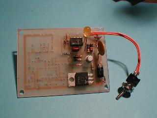
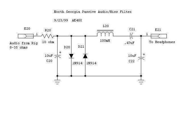
Your completed NoGaPiG should resemble the circuit in the above photograph. The NoGaPiG board has been designed to allow you to make modifications to the basic circuit, as well as providing board space and traces to construct a TiCK (using Embedded Research's TiCK chip) or a K8 (using K1EL's K8 chip) keyer and a popular audio hiss filter.
Add a Low Voltage Drop Schottky Diode in series with the power source. You may feel more comfortable with a diode in series with the power source (if the voltage source is reversed, current cannot flow). You can install a Schottky diode at the spot marked "D0," and cut the trace between the pads where the diode leads are soldered. This will not affect any other functions of the NoGaPiG.
Bypass the Voltage Monitor. You may wish to eliminate all extraneous power consumption. The low voltage monitor runs constantly and uses about 4-7mA. The trace marked "SW2" can be cut and a SPST Switch installed to cut off the OPAmp voltage comparator, the 5.1v zener reference, and the R3/R4 voltage divider. If you do this you will have to periodically close the switch to determine the battery condition. THIS IS NOT RECOMMENDED for the obvious reasons (i.e. why the need for the unit exists in the first place), but will reduce the total power consumption.
Board Ver A, Document Version 1.0
Submitted by Sam Billingsley, AE4GX
Since the North Georgia QRP Club shipped it's first kit in Oct 1999 we have kitted and sold almost all of the initial 100 kits that we planned. We are now accepting orders for the second hundred PiGs.
(UPDATE: 7/22/2003) We have now shipped over 400 kits. There is no shortage of parts so we plan to have this kit available indefinitely. J. Pickett Cummins, AD4S
This was our first club kit and we suffered like most from trying to hurry out the product to the QRP community. Frankly we have had almost 100% responses as good to excellent. Only one kit I'm aware of was damaged during mailing. We have identified some corrections to the Doc. Ver 1.0 manual that may help others avoid construction problems. Although most builders have worked through these problems without major trouble.
NOGAPIG Errata Ver. 1.0, January 15, 2000
************* end of NOGAPIG errata Ver 1.0 1/15/2000
The primary purpose of the PIG is to monitor your battery voltage and let you know via an illuminated LED that the minimum threshold has been reached. The condition is detected by comparing a 5.1 Volt zener with the battery voltage being supplied to a voltage divider formed by two resistors in series. The conjunction of these two resistors is the other reference along with the zener voltage to an OpAmp voltage comparator.
As long as the battery is high enough to exceed the zener as at the common point of R3 and R4 then the LED tied to the output of the OpAmp remains off. When the voltage at the R3/R4 common point drops below the zener value then the voltage comparator brings the output low and the LED lights indicating reaching the LOW VOLTAGE threshold point. You can then take what action you need (i.e. swapping batteries, paralleling another with the current one, etc.).
The PIG is shipped with three components that determine the threshold point. The zener at 5.1 Volt 5%, R3 10K Ohms and R4 8.2K Ohms. With these values at their nominal values the LOW VOLTAGE threshold will occur at about 11.3 Volts.
The set point can be easily changed by altering one or more of the three values. The simplest way is to change one of the two resistors. Below are standard resistor values and expected thresholds given a 5.1 Volt Zener.
| R3 | R4 | Set Point (Volts) |
| 10K | 8.2K | 11.3 |
| 12K | 8.2K | 12.6 |
| 10K | 6.8K | 12.6 |
| 11K | 8.2K | 11.9 |
| 10K | 7.5K | 11.9 |
| 100K | 82K | 11.3 |
| 100K | 75K | 11.9 |
| 100K | 68K | 12.9 |
If you are really tight with your current usage you may want to use larger values to reduce the current to an absolute minimum. The supplied resistors use about 0.5 mA (very small as is).
To set the set point to a specific value that is not attainable using standard resistor values you can put a single turn resistor trimmer on the board and replace the R3 and R4 locations with wire jumpers. Again the higher the basis value of the POT the smaller the current consumption. There are two traces to cut in the POT location to activate it's use. See the board etch layout and schematic for component locations.
BTW, there is a great undocumented (in the current manual) feature regarding this low voltage detection. As the battery is discharged via normal operation there will be a point that the RX battery drain is above the threshold and the TX battery drain pulls the voltage below the set point. When this happens the LED begins turning on and off and the Morse rate and the light follows the code. As the voltage continues to drop eventually the LED will light the entire time the TX is occurring and go off on RX. Later the RX alone will pull the voltage over the set point and the LED will stand on. These changes are most noticeable with the smaller current capacity batteries and the good news is that's the ones you need to watch the most. So you get a little LED flashing attractor to help you notice the low voltage event as a bonus.
We had intended to put a note in the first kit release but missed it in the QA. When we had the first boards made we used a 6-32 hole size (probably should have used X-40 size hole) and put it too close to the traces particularly the battery plus supply buss point when we moved to the production phase.
The hole itself is OK but when you put the nut and possible washer on it overlaps with the trace. So if you are mounting you PIG using metal standoffs or brackets you may need to file off the corner of the plus buss next to the mounting hole. This section is not used unless you install an optional in-line Schottky diode. (Not really needed but we thought some folks would want the capability to install the extra insurance). The easy way is to cut the plus buss trace between the top buss pad of the Polyfuse (F1) and the corner pad of the board. The other three corners are also very close to the ground trace that runs around three sides of the board.
Typically the user's enclosure is at ground potential so this should present no real problem. However, you should reroute this ground trace at the corners with small gauge wire jumpers to bridge the edges a little further away from the mounting holes and remove the section of the trace adjacent to the hole.
Sam/AE4GX
The NOGA team has been working with several PIG buyers who have reported a condition where the SCR falsely trips (i.e. falsely indicating an over voltage condition). This can occur just after hooking up a normally charged gel cell (approximately 12-13V).
If you haven't built your PIG, or are experiencing this problem described above after building your PIG, add a 1uF (included in production run 2 and later kits) or greater electrolytic across the output pads of the PIG (i.e. the pads where the load is connected). If no indication of false tripping exists then this modification should not be necessary. However, it will not hurt to do it as a precaution.
The story behind the diagnosis and resolution of this problem is actually quite interesting. Read the email dialog at http://www.qsl.net/~nogaqrp/. It was quite a lengthy process and shows the great diligence and determination of QRPers who are there looking for new "working" tools to use with their gear. Don, K5KW, Bob, WA1EDJ, and others namely BIGBOB97 have provided detailed information on the problem and helped eliminate extraneous test paths.
Thanks for your patience and understanding that these club kits (particularly the first) is a learning experience for us all.
Sam, AE4GX
The PiG keyer circuit is based on the K1EL, K8+, design. There are several sources for the 8 pin Microchip products that will work in this design. Both K1EL and Embedded Research can supply the chips. Complete documentation is available on the K1EL web site.
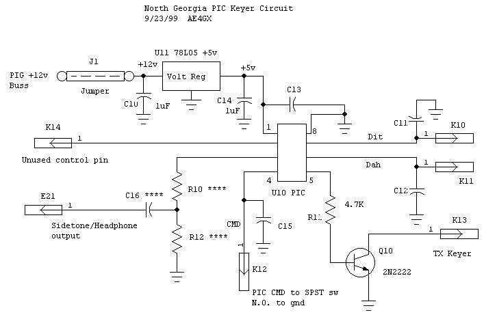
As you can see from the schematic, there are very few parts involved. Several PiG builders have installed a piezo buzzer (RS) instead of the audio output to the receiver's side tone. You can install a SPST switch to turn the buzzer off and on. This way you can program the chip without having a receiver hooked up.
Some of the capacitors in this circuit may be redundant since most builders will be bringing regulated voltage via the J1 jumper. We recommend them for safety and stability in an RF environment.
One problem has been found for this circuit on the version A PiG board. Both C10 and C14 are connected to the input of the 78L05, U10, 5v regulator. An easy fix is to swing the POS lead of C10 around and tack it to the output of U10.
Parts List
| U10 | Microchip 12C509 | |
| U11 | 78L05 +5v regulator | |
| C10,C14 | 1uF tantalum or electrolytic | |
| C13,C11,C12,C15 | .01 uF ceramic disk | |
| R11 | 4.7K 1/4 watt | |
| Q10 | 2N2222 NPN | |
| R10, R12, C16 | chose for desired waveshape to feed audio chain in receiver. | |
| 1 8-pin DIP socket | ||